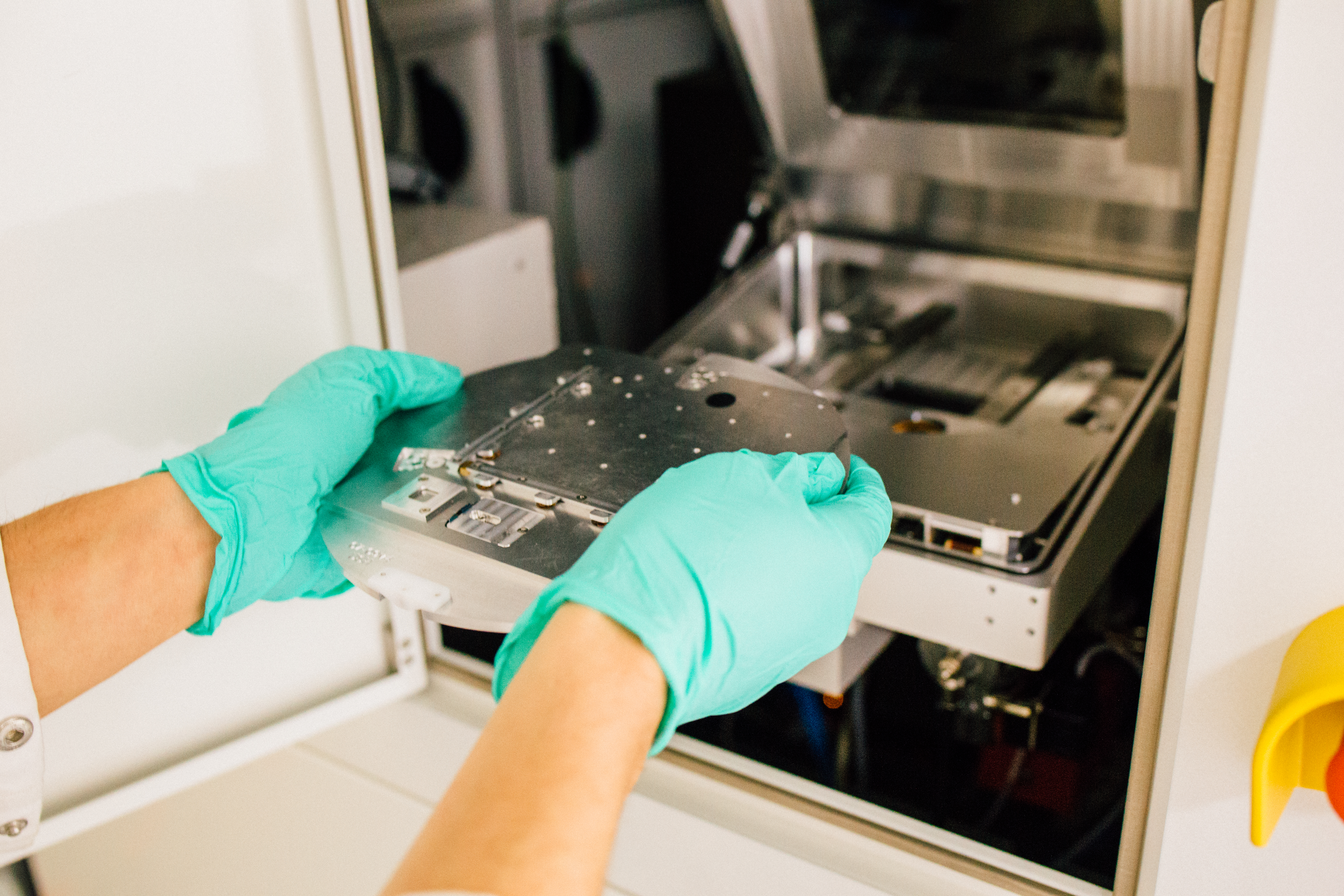
Femtosecond Laser Lithography System
- Post by: admin
- 1:45PM Oct 02, 2017
- Comments off
A lithography system designed with rapid prototyping capabilities in mind. This system allows for direct (mask-less) photolithography with the enhanced resolution enabled by a two photon absorption writing process. This process allows for writing of 3D structures with resolutions down to 1m.
Two photon absorption photolithography allows mask-less patterning because of its directionality. The light incident on the surface is at a wavelength of 780nm, meaning stray light does not expose the resist, as the photons are not individually energetic enough and exposure only happens in areas of very high intensity where it is possible for the resist to absorb two photons simultaneously.
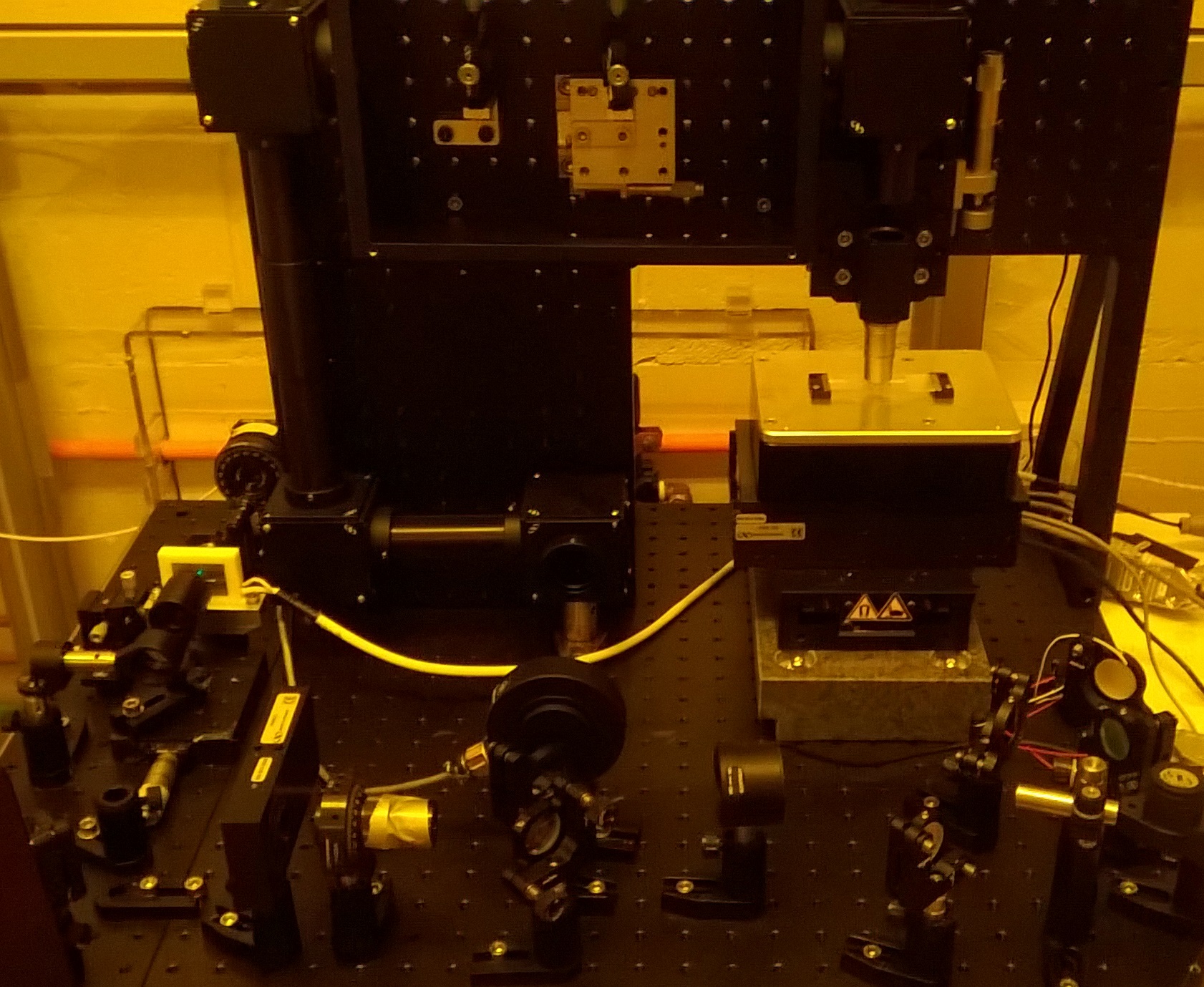
A custom built laser provides this light source. An all in fibre cavity produces mode-locked pulses at a repetition rate of 50MHz and a wavelength of 1560nm. These pulses are then amplified and frequency doubled to 780nm using a periodically poled lithium niobate crystal. The resultant output has an average power of 13mW and a pulse length of 70 fs. These ultrashort pulses therefore have very high peak power of 3.5kW and a pulse energy of 0.26nJ. By focusing these pulses onto a sample with a 40X microscope objective we can obtain peak intensities
Femtosecond Laser Lithography System
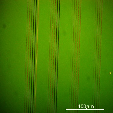
Lines written in AZ6612 positive photoresist with varying doses
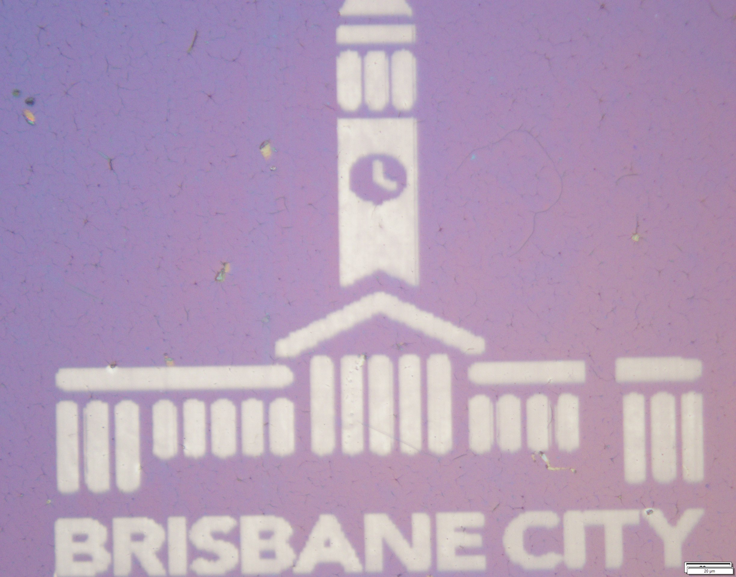
Laser reduction of graphene oxide (dark areas) to directly pattern graphene (light areas).
The lithography is controlled by the nFab software from Newport. The software has accurate power and write speed control as well as a fast shutter to allow delivery of well controlled average write intensity. A telescope in the beam path allows for control of the beam spot size and a camera provides real time images of the writing process. The write field area is 150mmx150mm with an accuracy of ±10nm and programmable focus correction. 2D or 3D patterns in several formats can be imported into the software for writing.
The combination of low average power and high peak intensity are useful for localised multi (n>2)-photon absorption processes without unnecessary heating. One application of this is the direct laser writing of graphene structures. A substrate coated with graphene oxide can be exposed under this system, and the high peak intensity efficiently reduces the oxide to graphene. This allows low cost rapid prototyping and production of devices based on graphene, a material used in a large array of applications from sensing to power storage.
Femtosecond lasers are excellent tools for a range of materials processing tasks including direct writing of optical waveguides, 2D and 3D photonic crystals and opto-mechanical and opto-fluidic devices.