Raith150 Two Electron Beam Lithography System
- Post by: admin
- 12:43PM Oct 02, 2017
- Comments off
The Raith150 Two (https://www.raith.com/products/raith150-two.html) is a versatile electron beam lithography system which can be used for patterning measurement and imaging of samples down to a few nanometres (~10 nm). Our system is compatible with arbitrary small samples and fragments, while at the same time being able to process wafers up to 6 inch. A very wide range of organic and non-organic materials can be processed and custom-made designs can be pattern on the desired sample surface. We have currently developed two main processes:
- the patterning of aluminium electrodes.
- the fabrication of chromium photonic crystal structures.
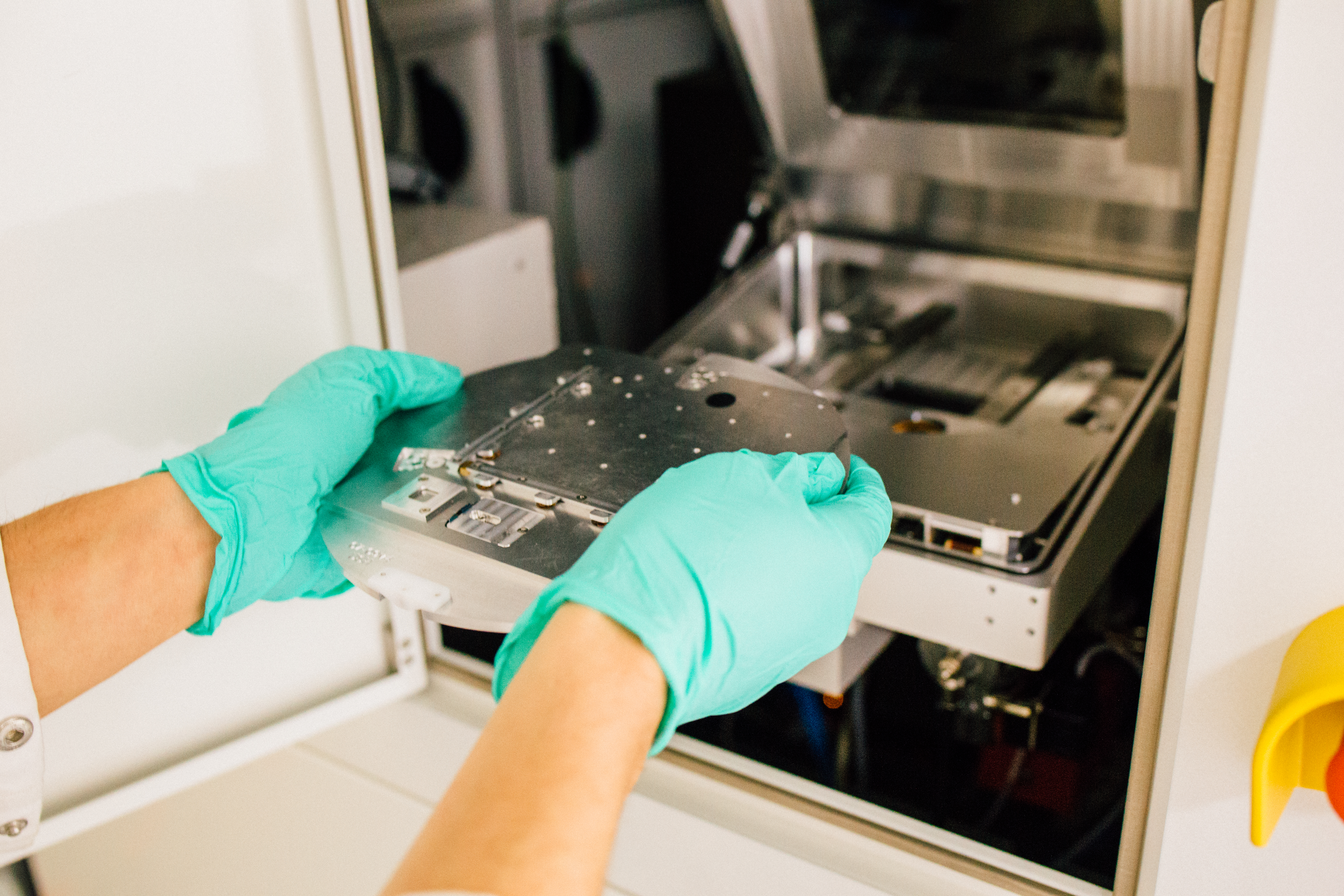
Loading of a wafer in the Electron Beam Lithography system.

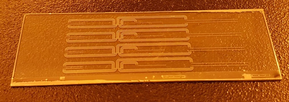
An example of one of our chips with four sets of electrodes.
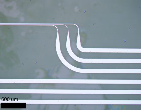
ur electrodes are defined on top of proton exchanged waveguide diffused in a lithium niobate wafer. For EBl standards, these structures are wide (~10 um) and extremely long (cms scale) but we are able to consistently obtain precise overlay alignment over the full size of the pattern. With these electrodes we can take advantage of the very high electro-optic coefficient of LN to produce reconfigurable optical circuits for both classical and quantum applications.
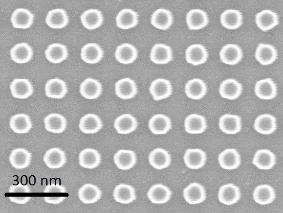
We are also capable of defining and etching chromium photonic crystals on the surface of LN. So far we successfully fabricated structures with periods down to 200 nm, with a wide range of base geometries ( e.g. circles, squares and hexagons). The purpose of this structures is to enable the enucleation of poled nanodomains and to study the plasmonic properties of these surface structures.
Array of photonic crystals with a circular base geometry.