Lithium Niobate Waveguide Fabrication Facility
- Post by: admin
- 6:01AM Oct 03, 2017
- Comments off
Lithium Niobate is a material with outstanding optical properties, including a wide transparency range spanning from UV to mid-infrared wavelengths and one of the highest nonlinear and electro-optic coefficients among all the known ferroelectric materials. Waveguides fabricated on this substrate, by confining light over large distances, can enhance by several orders of magnitude the efficiency of optical nonlinear processes and find numerous applications in both classical and quantum information, e.g. optical frequency conversion, generation of single photons, and fast electro-optic modulation.
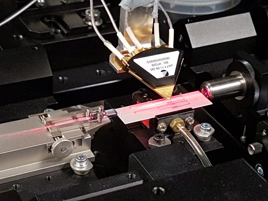
In our facility we have the capability of fabricating all of these components starting from bare Lithium Niobate wafers. Our technology of choice for the realization of integrated circuits, called Reverse Proton Exchange, enables low propagation losses (<0.1 dB/cm) at telecom wavelength as well an high coupling efficiency (≈90%) with optical fibre, making our waveguides an ideal interface for the development of hybrid quantum technologies.
The fabricated waveguides can be used for efficient frequency conversion or single-photon generation processes after periodic reversal of the spontaneous electric domains of the crystal through the application of a strong electric field (periodic poling). Our poling setup can achieve periods smaller than 10 microns and enable frequency conversion at wavelengths as small as 370 nm.
Electro-optically reconfigurable circuits are fabricated by depositing metal electrodes on top of the waveguides to actively control their refractive index. With our capabilities we can reach modulation speeds as high as 1 GHz and fabricate complex reconfigurable networks with up to 10 output channels in a compact and stable architecture.
Waveguide chip fabricated in our facility
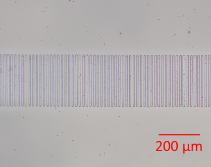
Periodically poled domains revealed by HF etching
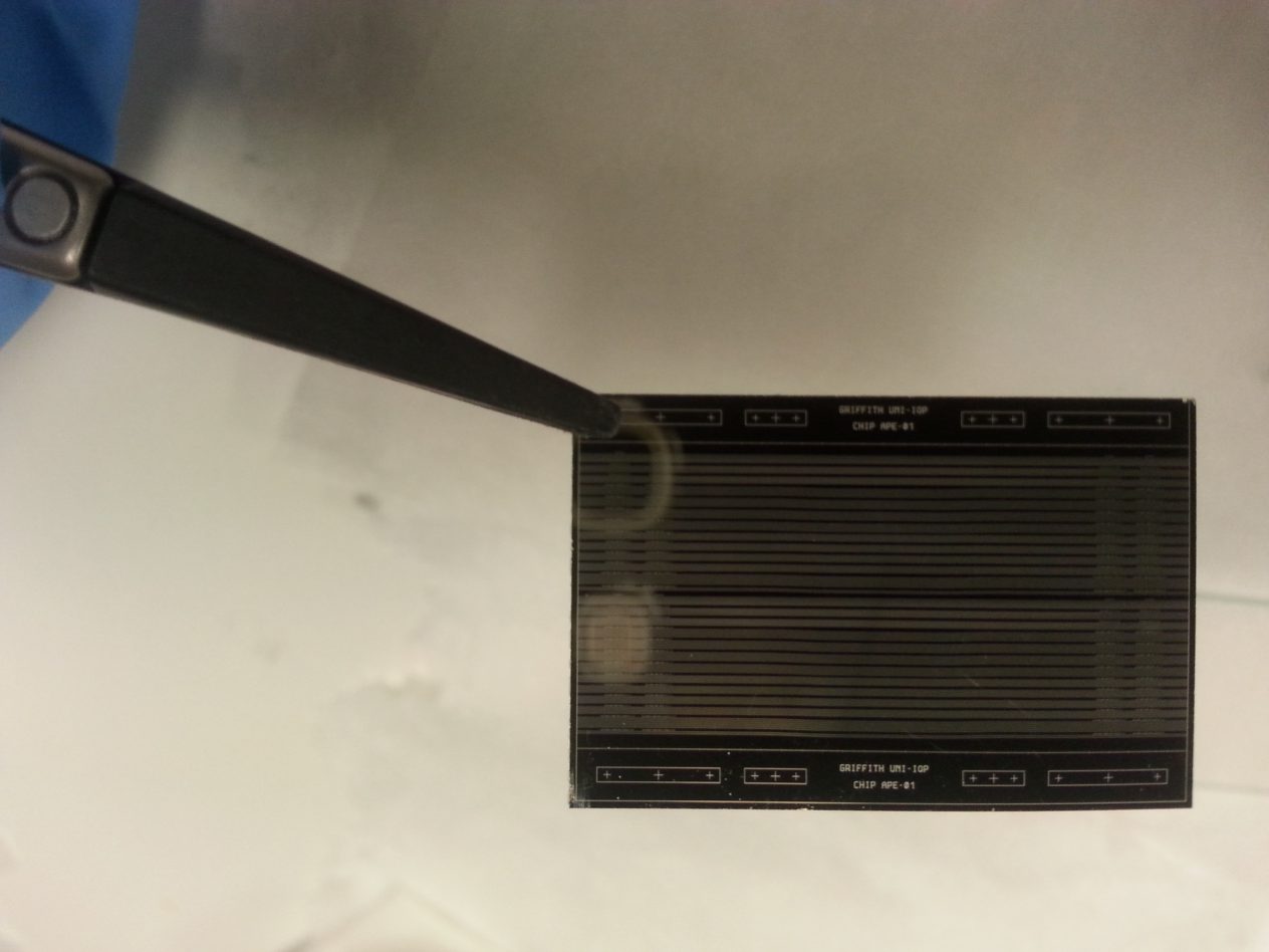
Photograph of an electro-optically reconfigurable waveguide chip